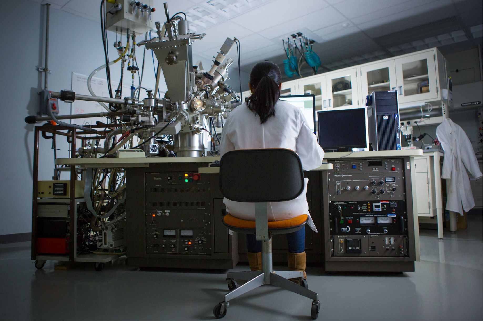
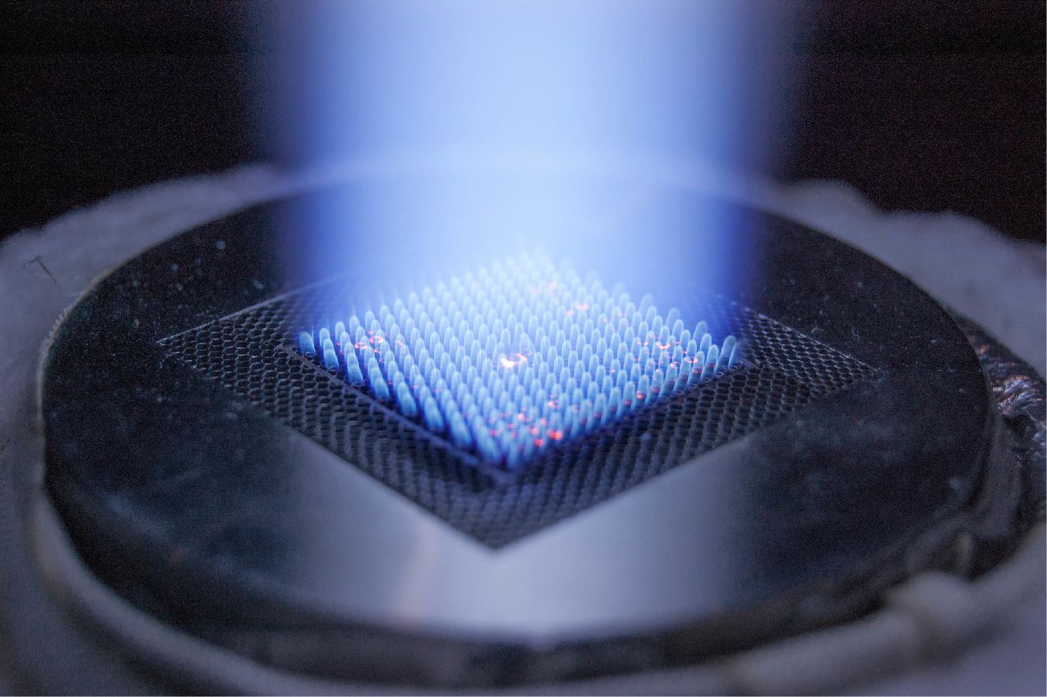
Huge resources of unconventional gas are locked up in tight-gas sands in the Gulf of Mexico (GOM), Rocky Mountains, Texas, Oklahoma, and the Appalachian Basins. However, there are still large cost and technological hurdles to over-come before significant quantities of gas can move from the possible resource category to proved developed producing (PDP) reserves. A considerable amount of this gas is in deep (>15,000 feet) reservoirs. Recently a major oil company announced plans to drill in excess of 30,000 feet below the mudline on the continental shelf of the GOM. The drilling environment at these depths will be high pressure (approaching 30,000 psi) and high temperature (> 600°F or 316°C).
Efforts to adapt the capabilities and reliability of logging while drilling (LWD), measurement while drilling (MWD), other logging tools, and other “smart well” tools to high temperature (HT) and high pressure (HP) conditions have been underway for some time. Prior to the current Deep Trek program, the National Energy Technology Laboratory (NETL), Maurer Engineering Inc., Sperry-Sun, and Halliburton Energy Services recognized the future need for HT drilling and geological measurement technology. In 1997, these parties entered into a partnership to enhance the capabilities of HT LWD and MWD tools. The goal for the LWD project was to extend the temperature range from 140°C (284°F) to 175°C (347°F) with survivability to 200°C (392°F). The goal for the MWD project was to extend the temperature range from 175°C (347°F) to 195°C (383°F). Both projects had limited success in meeting their objectives.
The results from these two projects and other industry input made it evident that current electronics are not capable of providing the building blocks needed to develop the tools necessary to characterize reservoirs and drill complex wells in HT/HP environments. As a result, the Department of Energy’s Office of Fossil Energy and NETL have partnered with industry to encourage the development of HT electronic component building blocks. This initiative will enable the electronics industry to provide the component production infrastructure needed by the oil and gas industry to develop the advanced electronic tools needed.
This project began with the proposed objective of delivering an 80186 Micro-controller and conducting a High Temperature Demonstration, as well as some additional products. Once the JIP convened, priorities were re-evaluated and re-negotiated with the DOE. This revised program is developing an Electrically-Erasable Programmable Read-Only Memory (EEPROM); a Re-Programmable (volatile) field-programmable gate array (FPGA); a Precision Operational Amplifier (OpAmp), a Sigma-Delta A-to-D Converter (ADC); and an 0.8 Micron High Temperature Mixed Signal Process (HTMSP) and Tool Kit.
Results
The project has resulted in the successful design and testing of four key components needed for high temperature drilling equipment. These include: an Electrically-Erasable Programmable Read-Only Memory (EEPROM); a Field Programmable Gate Array; a Precision Amplifier (OpAmp) and a Sigma-Delta Analog-to-Digital Converter (ADC). The establishment of a Joint Industry Project (JIP) and participating companies’ commitment was a major reason for the project success. Major results include:
- Applied Honeywell advanced SOI technology adapted from Aerospace/Defense applications
- To develop an IC foundry process for HT electronics, which is complete and in production.
- To develop models, libraries & toolkits for HT Mixed-Signal ASICs, which are complete and are used to develop mixed-signal chip with 90K gate & custom analog drop-in.
- Developed and commercialized high-priority functions to 225°C specifications
- Precision amplifier - Complete, verified and sampled. 1st pass success
- Field Programmable Gate Array (FPGA) - Complete, die level verification, 1st pass success
- High-resolution A-to-D converter - 2nd pass design, layout and fabrication complete
- Non-volatile memory (EEPROM) - Demonstrated EEPROM data retention and durability via 32Kbit test-chip; 256Kbit product design, layout and fabrication complete
Benefits
The HT components developed in this project will benefit a wide range of industries, as well as the primary stakeholders within the oil and gas industry. Significant gas resources in the U.S. are in deep, HTHP reservoirs. A number of these gas reservoirs may have temperatures greater than 450° F (232°C), with some exploration wells expected to see temperatures approaching 500°F (260°C) or more. The current electronic technology (memory chips, processors, etc.) cannot operate at these conditions. The purpose of this project is to develop basic electronic chips deemed very important by the JIP, as well as their associated manufacturing and programming, which will provide the building blocks needed to build sophisticated sensors and tools to reliably, efficiently, and economically drill and produce from hot deep (to 20,000 feet and deeper) depths.
Summary
The twelveth and final meeting of the JIP was held in Plymouth, MN on July 17,, 2007. At that time the project was 99% complete and then was completed July 31, 2007.. The results of the project include applying Honeywell’s advanced SOI technology adapted from Aerospace/Defense applications to develop an IC foundry process for HT electronics, and to develop models, libraries & toolkits for HT Mixed-Signal ASICs for use to develop mixed-signal chip with 90K gate & custom analog drop-in. The project also included the development of the four chips, whose features are listed below:
- HTOP01: Precision Amplifier
- Die size: 2.3mm x 1.8mm
- Dual amplifier
- Continuously auto-zeroed
- Very low offset and noise
- High Temperature FPGA
- Die size: 16.1mm x 12.0mm
- SRAM based, re-programmable
- 32K gates, up to 204 user I/O
- ATMEL AT6010 equivalent
- High Temperature 256-Kbit EEPROM
- 5 V Operation, ± 5%.
- -55 °C to 225 °C temperature range (250°C die temperature)
- Read and write over full temp. range
- 5 year reliability
- 10,000 data write cycles (goal), 1,000 cycles for sure
- 1,000 hour intrinsic (no refresh) data retention at 250°C die temp.
- Read access: < 200 ns
- Available as parallel or serial interface, modeled after industry 28C256 and 25C256 components (configure by pad connection)
- Includes FPGA configuration loader
- Incorporates EEPROM High Temperature Data Management
- 5-year data retention at >225C with periodic refresh (re-write)
- Refresh hand-shake request on POR (cleared after 20 seconds)
- Refresh hand-shake request at 30-day intervals
- Die size: 12mm x 12mm
- 18-bit A-to-D Converter
- 2nd Order S? Architecture
- 2048 oversampling ratio
- 45 Hz. bandwidth @ 204.8KHz clock
- On-chip digital filters
- 4-wire SPI Data and Control Interface
- Fully Differential Input and Reference
- Optional single-ended Input Mode
- 1-bit S? Modulator Data Output
- Supports Test & Off-Chip Digital Filters
- Single Pin Clock Selection (Internal Oscillator or External Clock)
- On-Chip 1.5 V Precision Voltage Reference
- PTAT Current Source Output
- Matched Reference Current Source Outputs
- Auxiliary 8-bit ADC (Successive Approximation)
- Temperature Measurement via Built-In 8-bit ADC (~1.4 °C resolution)
- Low Current Sleep State When Not Performing A-to-D Conversion
- -55 °C to 225 °C specified operation
- Single Supply 5V Operation
- Binary or 2’s complement output
- Die size: 10.2mm x 9.5mm
Also, due to budget shortfalls for the project, Honeywell has internally funded commercialization tasks associated with the four chips, including:
- HTADC18 and HTEEPROM prototype wafers to bring lot size to minimum required for fabrication
- HTADC18 wafer-level reference / oscillator trim program
- Initial assembly and functional test
- HTEEPROM wafer-level test hardware
- HTEEPROM preliminary package design
- Product introduction planning


