Business

News and Events
Research and Programs
Business
The goal of this project is to develop and qualify a Re-configurable Processor for Data Acquisition (RPDA) by packaging previously developed components in an advanced high-temperature Multi-Chip Module (MCM), and by developing configuration software that may be embedded within the RPDA to link data-acquisition system Analog Front-Ends to digital system busses.
Honeywell International Inc., Plymouth, MN 55441
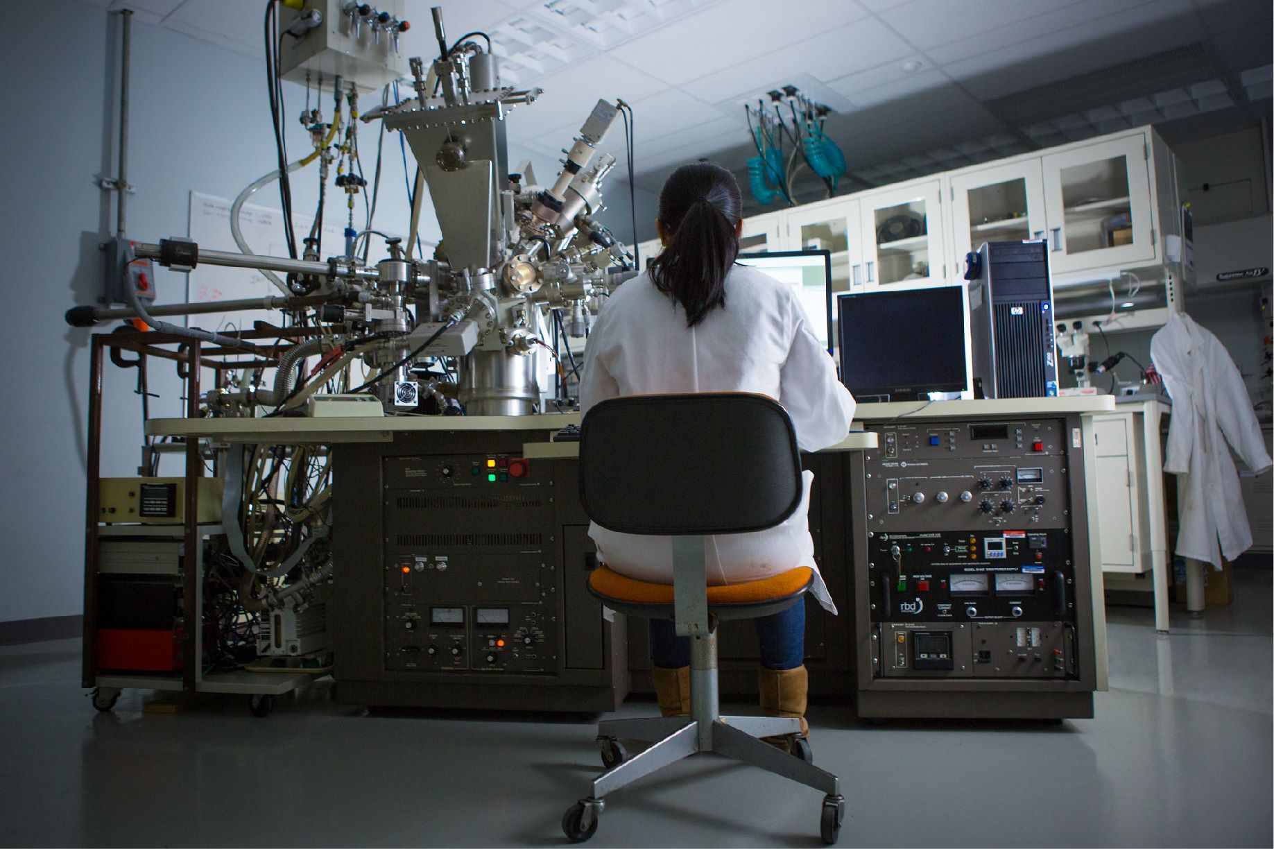
Electronic data acquisition systems are necessary to make deep oil and gas drilling and production cost effective, yet the basic electronic components from which such systems are built will not operate reliably at the high temperatures encountered in deep wells. As well depths increase beyond 15,000 feet, temperatures above 200°C are relatively common. In some cases the target reservoir temperature may be as high as 300°C.
Deep oil/gas reservoirs are not being developed for lack of data acquisition tools that handle the high temperatures encountered in wells at great depths. A previously awarded Deep Trek HTE project has established that viable high temperature electronics technology exists for 250°C and above, and is available now. Components developed under that program have validated the usefulness of that technology and provide several key building blocks for down-hole data acquisition systems. These components help to overcome some of the most challenging development obstacles and help to stimulate further interest in high temperature electronics by demonstrating feasibility and enabling rudimentary systems.
This project will further stimulate research and development interest in high temperature electronics, and foster the application of the previously developed components into down-hole tools. Furthermore, since the goal of this project is a re-configurable solution, the hardware developed within this project can be applied to other applications, including down-hole data processing, actuator controls, pulse-width modulator controls for DC-to-DC converters and other applications which may result once down-hole tool makers realize the flexibility and capability of this approach. A re-configurable solution will enable them to develop new digital control, processing, and utility components without requiring them to have any significant expertise in integrated circuit development. This flexibility will enable these components to adapt themselves to the Analog Front-end interfaces resulting from current and future high-temperature integrated circuit development. The programmability will eliminate delays otherwise required by IC design and fabrication cycles, enabling customization on a tool-by-tool basis. Nothing like this level of capability and flexibility has ever existed within a single hardware component for high-temperature environments such as down-hole oil and gas exploration.
The project is divided into two phases, During Phase I, which is now complete, detailed development plans have been finalized, the RPDA package design, has been completed, FPGA functional configurations have been developed, and the overall test plan and procedures have been outlined and documented. The RPDA design objectives specification has been delivered. This document identifies high-level requirements, targeted applications information, physical design, and preliminary specifications. It covers those aspects of the RPDA that define form, fit and function (such as sub-components, physical dimensions, electrical interfaces, operating conditions, and functional capabilities). This document addresses the RPDA requirements for an un-configured device as well as the requirements for a specific functional configuration.
This project began in October 2006. A Research Management Plan and Technology Status Assessment have been completed. Additionally, the RPDA design objectives specification and a preliminary package design covering dimensions, internal component specification and placement, package materials, and connectivity, have been completed. The design provides for a high-level of test coverage for the internal components. The completed design contains a static random access memory (SRAM), a field-programmable gate array (FPGA), a non-volatile memory (high-temperature electrically erasable programmable read-only memory), and capacitors associated with the use of these high-temperature integrated circuits. FPGA simulation databases have been developed, and trial FPGA configurations have been simulated.
During Phase II, prototype RPDA units will be fabricated, configured, and tested, including complete characterization of configured functionality at high-temperature (225oC minimum).
(July 2009)
Phase I activity has been completed, and the Phase 1 final report was delivered in October 2007.
Phase II is in progress. This phase focuses on fabrication and demonstration of prototype units. Ceramic packages have been fabricated in conformance to the requirements defined during Phase 1. These packages are designed to house all three of the RPDA integrate circuits (FPGA, EEPROM, and SRAM) and supporting components (capacitors) in a single, ruggedized package that incorporates embedded electrical routing and connections between the die and out to the package pins.
Die-level testing completed during Phase II revealed that a design revision was required for the High Temperature EEPROM to correct some errors in the signal routing and logic design of that integrated circuit. Those design changes have been implemented in a Pass 2 EEPROM design and additional integrated circuit wafers have been fabricated for program use. Demonstration units will be assembled using the revised High Temperature EEPROM along with the other die (FPGA and SRAM). Demonstration hardware will be tested to verify hardware connectivity, and to demonstrate configuration of the RPDA via configuration files programmed into the EEPROM.
Honeywell has completed the development of the Re-configurable Processor for Data Acquisition (RPDA) thus completing the technical requirement for this project. The Final Project Report is available below under "Additional Information".
$773,522
$280,251
NETL – William Fincham (william.fincham@netl.doe.gov or 304-285-4268)
Honeywell – Bruce Ohme (bruce.ohme@honeywell.com or 763-954-2189)
Final Project Report [PDF-3.25 MB]
Phase I Final Report [PDF-1.37MB]
Technology Status Assessment [PDF-92KB]